Ⅰ. Introduction
After the 1950s, four basic processes (ion implantation, diffusion, epitaxial growth, and lithography) were invented, and the semiconductor IC process was gradually developed. It is simple to harm the circuit function in the chip if it is polluted by dust particles and metals, generating a short circuit or open circuit, etc., resulting in the failure of the the production of geometric characteristics. As a result, in addition to avoiding external pollution sources throughout the production process, wet or dry cleaning is required for integrated circuit fabrication procedures such as high temperature diffusion and ion implantation. Dry and wet cleaning work involves using chemical solutions or gases to successfully remove dust, metal ions, and organic impurities that have remained on the wafer while preserving the wafer's surface and electrical properties.
Ⅱ. Classification of pollutants and impurities
Some organic and inorganic compounds are required in the IC fabrication process. Furthermore, the manufacturing process is always carried out in a clean room with human intervention, resulting in various environmental pollution of the silicon wafer. Pollutants are classified into four categories based on their occurrence: particles, organic matter, metal pollutants, and oxides.
2.1 Particles
Polymers, photoresists, and etching impurities make up the majority of the particles. Typically, the particles stick to the silicon surface, impacting the subsequent process' development of geometric features and electrical properties. Although the adhesion between the particles and the surface is diverse, it is primarily attraction, thus the particle removal method is primarily to undercut the particles using physical or chemical ways, and gradually remove the particles. The particle's contact area with the silicon surface is reduced, and the particles are eventually removed.
2.2 Organics
Human skin oils, clean room air, mechanical oils, silicone vacuum greases, photoresists, cleaning solvents, and other organic contaminants can all be found in the IC process. Each contaminant affects the IC process in a different way, mainly by producing an organic layer on the wafer surface that prevents the cleaning solution from reaching the wafer surface. As a result, removing organic materials is frequently the first step in the cleaning procedure.
2.3 Metal contaminants
Metal interconnect materials are utilized to connect separate devices in the IC circuit fabrication process. Photolithography and etching are used to create contact windows on the insulating layer, and then evaporation, sputtering, or chemical vapor deposition are used to create metal interconnects (CVD). To construct interconnect lines, interconnect films such as others are etched, and then the deposited dielectric layer is chemical mechanical polished (CMP). This procedure has the potential to contaminate the IC production process. Various metal contaminations are produced while constructing metal interconnects. To remove metal pollution, appropriate steps must be done.
2.4 Primary oxides and chemical oxides
In an environment including oxygen and water, silicon atoms are very easily oxidized to create an oxide layer, known as a native oxide layer. Due to the great oxidizing power of hydrogen peroxide, a chemical oxide layer will form on the silicon wafer surface after cleaning with SC-1 and SC-2 solutions. This surface oxide must be removed once the wafer has been cleaned to assure the quality of the gate oxide. Oxides produced by chemical vapor deposition (CVD) in the IC process, such as silicon nitride and silicon dioxide, should also be selectively removed in the cleaning process.
Ⅲ. Classification of cleaning methods
3.1 Wet cleaning
Wet cleaning oxidizes, etchs, and dissolves wafer surface contaminants, organic debris, and metal ion contamination using liquid chemical solvents and DI water. RCA cleaning, dilution chemical cleaning,cleaning, single wafer cleaning, and other wet cleaning procedures are commonly employed.
3.1.1 RCA cleaning method
People did not utilize a regular or systematic method of cleaning at first. The RCA cleaning process for silicon wafer cleaning was invented by RCA (Radio Corporation of America) in 1965 and applied to the manufacture of RCA components. This cleaning procedure has since been the foundation for many front and rear cleaning processes, and most manufacturers' cleaning processes will be based on the original RCA cleaning method in the future.
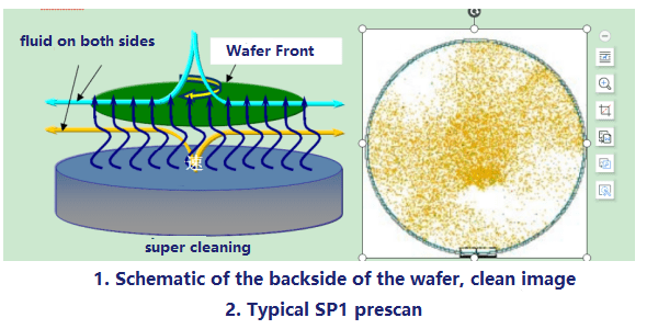
To spray, clean, oxidize, etch, and dissolve wafer surface contaminants, organics, and metal ion contamination without harming wafer surface characteristics, RCA cleaning uses solvents, acids, surfactants, and water. After each chemical usage, thoroughly rinse in ultrapure water (UPW). The purposes of some of the most regularly used cleaning fluids are listed below.

Figure. 1
(1) APM (NH4OH/H2O2/H2O at 65–80°C) is an ammonium hydroxide/hydrogen peroxide/DI water mixture. The formula for APM is NH4 OH:H2O2:H2O=1:1:51:2:7, with oxidation and micro-etching to undercut and remove surface particles; also can remove light organic contamination and some metalized pollution. Surface roughness, on the other hand, develops simultaneously with silicon oxidation and etching.
(2) A mixture of hydrochloric acid, hydrogen peroxide, and DI water (HPM; HCI/ H2O at 65–80°C). HPM is also known as SC-2 cleaning solution, and its formula is as follows: In addition, chloride ions in hydrochloric acid undergo a complex reaction with residual metal ions to form complexes that are easily soluble in aqueous solution, which can be obtained from HCI: :H2O=1:1:61:2:8, which can dissolve alkali metal ions and hydroxides of aluminum, iron, and magnesium, in addition, chloride ions in hydrochloric acid undergo complex reaction with residual metal ions to form complexes that Metal pollutants are removed by the bottom layer of silicon.
(3) Sulfuric acid (sulfuric acid)/hydrogen peroxide (hydrogen peroxide)/deionized water (DI water) mixture (SPM; H2O2/ H2O at 100°C). SC3 cleaning solution is another name for SPM. Sulfuric acid and water have a volume ratio of 1:3. It's a common cleaning solution for getting rid of organic contaminants. Organic matter can be dehydrated and carbonized with sulfuric acid, whereas carbonized goods can be oxidized with hydrogen peroxide to produce carbon monoxide or carbon dioxide gas.
(4) Etching with hydrofluoric acid (hydrofluoric acid) or diluted hydrofluoric acid (diluted hydrofluoric acid) (HF or DHF at 20 to 25 degrees Celsius). Its formula is HF:H2O=1:2:10, and it's used to remove oxides from hard-to-reach places, etch silicon dioxide and silicon oxide, and decrease surface metal. After SC1 and SC2 solution cleaning, a diluted hydrofluoric acid aqueous solution is utilized to remove the native oxide layer and a chemical oxide layer created by the oxidation of hydrogen peroxide on the wafer surface. Silicon hydrogen is produced on the surface of the silicon wafer as the oxide layer is removed. bind together and form a hydrophobic surface
(5) DI water is another name for ultrapure water (UPW). After chemical cleaning, UPW employs ozonated water to dilute chemicals and rinse liquid for wafers.
After RCA cleaning incorporates megasonic energy, it may minimize chemical and DI water consumption, shorten the etching time of the wafer in the cleaning solution, reduce the impact of wet cleaning isotropy on integrated circuit characteristics, and increase the usage of the cleaning solution. life.

Figure. 2
3.1.2 Dilution chemistry
The dilution chemical approach for SC1 and SC2 mixes can save a lot of chemicals and DI water when used in conjunction with cleaning. The in the SC2 combination can also be eliminated completely. The APM SC2 mix can be diluted (1:1:50) to remove particulates and hydrocarbons from the wafer surface. In the removal of metals, strongly diluted HPM mixes (1:1:60) and diluted (1:100) can be as effective as conventional SC2 fluids. The fact that particles do not settle at lowconcentrations is another advantage of employing dilute HCl solutions. Silicon and silicon oxide are equal in potential because the ranges from 2 to 2.5. The surface of the silicon wafer has a network of negative charges if the value is greater than this point; the surface of the silicon wafer has a network of positive charges if the pH value is lower than this point. When the pH of the solution exceeds 2 to 2.5, the particles in the solution have the same charge as the silicon surface, forming an electrostatic shield between the particles and the silicon surface. This barrier can prevent particles from being expelled from the solution during the etching of the silicon wafer in the solution. deposited on the surface of silicon. However, because the wafer surface is positively charged and the particles are negatively charged at pH values below 2, there is no shielding effect, causing particles to deposit on the silicon surface when etched in solution. The HCL concentration can be effectively controlled to avoid particles in the solution from accumulating on the silicon surface. Overall chemical consumption is reduced by less than 86 percent when using the diluted leaning approach. The temperature of the solution in the tank can be reduced and the time of various cleaning steps can be optimized after diluted SC1, SC2 solution and HF supplemented with megasonic agitation, resulting in a prolongation of the solution's life in the tank and a reduction of chemical consumption by 80-90 percent. Experiments have shown that using hot UPW instead of cool UPW can save 75-80% on UPW use. Furthermore, due to low flow rates and/or cleaning time requirements, numerous dilution chemistries can save large amounts of flushing water.
3.1.3 IMEC cleaning method
The IMEC cleaning method is frequently used in wet cleaning to limit the usage of chemicals and DI water. Table 2 shows the IMEC cleaning method in action.
Organic pollutants are eliminated in the first phase, and a thin layer of chemical oxide is created to ensure efficient particle removal. Sulfuric acid combinations are commonly employed, however, ozonated DI water is used for environmental reasons, both to reduce chemical and DI water usage and to eliminate the more difficult sulfuric acid bath cleaning phase. With ozonated water, it is more difficult to entirely remove (hexamethyldisilazane), because ozone can be dissolved in high concentrations in solution at ambient temperature, but the reaction time is slow, resulting in incomplete HDMS removal. The reaction speed is accelerated at higher temperatures, while the dissolved ozone concentration is decreased, which impacts the scavenging effect. As a result, temperature and concentration parameters must be tuned in order to remove organic materials more effectively.
The oxide layer, as well as particles and metal oxides, are removed in the second phase. When metal ions such as Ag are present in the HF solution, they deposit on the Si surface. The deposition process is electrochemical, and under light circumstances, the rate of copper surface deposition is enhanced.
Metal ions are typically suppressed while oxide coatings and particles are removed using HF/HCL solutions. A modest number of chloride ions increases Cu deposition due to the catalytic effect in the +/Cu+ process, whereas a big amount of chloride ions is added to generate soluble high cuprous chloride synthesis. Copper ions are not deposited by the body. The adjusted HF/HCL mixture successfully prevents metal plating in the solution while also extending the solution's service life.
To avoid drying spots or watermarks, the third stage is to develop hydrophilicity on the silicon surface. To make the silicon surface hydrophilic at low pH without recontaminating metals, dilute HCL/O3 solutions are commonly utilized, and raising the concentration of during the final rinse lowers Ca surface contamination.
Table 3 shows a comparison of the IMEC cleaning procedure and the RCA cleaning approach.
The table shows that the IMEC cleaning process can achieve very low metal contamination while also being more cost effective due to its low chemical usage and lack of imprinting.
3.1.4 Single Wafer Cleaning
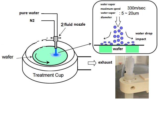
The above procedure cannot guarantee the completion of the cleaning process for large-diameter wafers. Cleaning is usually done with a single wafer, as depicted in the diagram below. Reusing DI-O 3/DHF cleaning solution at room temperature is the cleaning procedure. Dilute HF etches silicon oxide while eliminating particle and metal impurities, while DI water (DI-O3) creates silicon oxide. A brief spray period can achieve a satisfactory cleaning effect without cross-contamination, depending on the etching and oxidation requirements. DI water or ozonated DI water is used for the final rinse. Use isopropyl ethanol (IPA) mixed with a large amount of nitrogen for drying to avoid water stains. Improved RCA cleaning gives a better cleaning impact than single-wafer cleaning. Recycling of DI water and HF in the cleaning process reduces chemical consumption and improves wafer cost-effectiveness.
3.2 Dry cleaning
Dry cleaning removes impurities from the wafer surface using vapor-phase chemical techniques. Thermal oxidation and plasma cleaning are two of the most common gas-phase chemical techniques. The cleaning procedure involves introducing hot chemical gas or plasma reactive gas into the reaction chamber, where the reactive gas chemically combines with the wafer's surface to produce volatile reaction products that are vacuum evacuated. Table 4 lists the removal measures for various contaminants. In an oxidation furnace, annealing in a CI containment environment is a common thermal oxidation procedure, and argon (Ar) sputtering is commonly done in situ prior to sputter deposition.
Plasma cleaning involves the use of lasers, microwaves, thermal ionization, and other methods to convert inorganic gas into plasma active particles, which then combine with surface molecules to generate product molecules, which are then examined to form gas-phase residues that separate from the surface.
Dry cleaning has the advantage of leaving no waste liquid behind after cleaning and allowing for selected local treatment. The anisotropy of the dry clean etch also makes it easier to create delicate lines and geometric elements. The gas-phase chemical technique, on the other hand, is unable to selectively react solely with surface metal impurities and, as a result, reacts with the silicon surface. Varied volatile metal compositions have different evaporation pressures, and different metals have different low-temperature volatility. As a result, all metal contaminants cannot be totally eliminated under particular temperature and time conditions, hence dry cleaning cannot completely replace wet cleaning. Experiments demonstrate that metallized contaminants such as iron, copper, aluminum, zinc, nickel, and others can be reduced using gas-phase chemical techniques to meet the requisite criteria. Calcium can also be successfully volatilized at low temperatures using chemical techniques based on ions. Typically, a combination of dry and wet cleaning procedures is employed in the process.
Ⅳ. Summary
The most common process in the IC manufacturing process is semiconductor cleaning. The quality of the cleaning effect has a significant impact on the chip manufacturing process and integrated circuit properties. Improper handling of the cleaning solution's numerous components will substantially contaminate the environment, and a large number of cleaning cycles will consume a significant quantity of chemicals and DI water. Dilution chemical methods, IMEC cleaning methods, dry cleaning, and a combination of dry and wet cleaning methods can all help to decrease or eliminate the use of various chemicals and DI water. People are still studying more effective cleaning techniques, such as the effective matching of megasonic energy in the cleaning solution to remove sub-fine particles, in the face of IC processes with thinner scribe lines and higher integration. In higher precision IC operations,IC cleaning will confront increased problems.
- Prev:What is the Difference between DCS and PLC?
- Next:None
Suggested Resources
-
Phone
18126161077 -
Wechat


