In residential applications of a PV system, the most common system setup involves the following components: the PV panel, a pre-regulator (dc-dc converter) that also provides MPPT functionality, an interleaved boost converter (IBC), and a voltage source inverter (VSI) to guarantee the output current quality. The IBC, compared to a standard boost converter, provides ripple cancellation by forcing a 180° phase shift operation between the two switching cells. However, due to the high input voltage from the panels, the system suffers from high reverse recovery loss in the high voltage class silicon (Si) diodes (DB) and commutating loss in the switches (SB). The authors of this paper propose that the use of silicon carbide (SiC) diodes in the IBC will eliminate this loss owing to the zero reverse recoveries of SiC diodes.
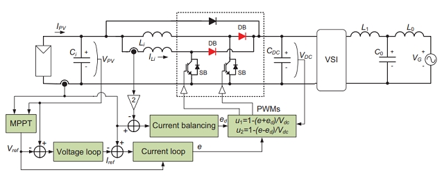
Fig 1. Two-stage PV inverter topology using a two-phase IBC with a conventional controller
The comparative study is conducted between two types of IBCs: one using SiC diodes (referred as Si/SiC system) and the other using Si diodes (referred to as Si/Si system). The study addresses the following issues: 1) the static and switching characteristics of two diodes with a CoolMOS device; 2) the efficiency of the system within the full operating range; and 3) the system power density.
A 2.5 kW hardware system was built for this study in which the measurement board, the main power board, the gate driving circuits, the CoolMOS devices, and the inductors were common for both Si/Si and Si/SiC systems. The main differences are the diode type, the component placement and the design of the cooling system. The cooling systems, which consisted of heatsinks and fan arrays, were set such that the junction temperature of the CoolMOS was maintained at 75°C for both the Si/Si and Si/SiC systems to minimize conduction loss. Similarly, the ambient temperature was maintained at 50°C for the duration of the experiment. The other parameters of the IBC are given in Table I.

Table I. Typical specifications of a pre-regulator (IBC) for a single-phase PV inverter
The CoolMOS, IPW90R120C3 by Infineon, was selected as the active switch. This device was chosen because of its sufficiently high breakdown voltage, low on-state resistance at low temperatures, which minimizes conduction loss, and high switching rates (di/dt and dv/dt), which minimize switching losses. The two diodes used were Si Ultrafast diode STTH1210D by STMicroelectronics and SiC Schottky diode C2D20120D by Cree.
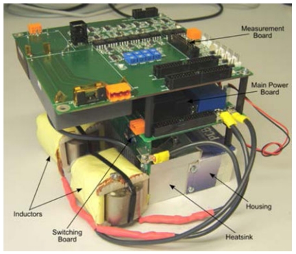
Fig 2. Optimized IBC setup
Ⅰ. Semiconductor Characterization and Cooling System Evaluation
Static and dynamic characterization is carried out for both the Si diode and SiC diode to determine their losses. Static characterization is used to ascertain the conduction loss of the devices. With the CoolMOS maintained at 75°C, it is found that the Si diode has a negative temperature coefficient, whereas the SiC diode has a positive temperature coefficient. As such, in higher current applications (> 2A), when the devices are heated, the conduction loss of the Si diode reduces, whereas that of the SiC diode rises.
Dynamic characterization of the two diodes was performed at 400V to determine their switching behavior and losses. After testing, it was found that the type of diode does not affect the turn-off performance of the CoolMOS device. However, a distinct difference was noted in the turn-on performance of the CoolMOS, which depends on the reverse recovery behavior of the diodes. The reverse recovery current increases the switching loss in the Si diode and reflects these characteristics on the drain current of the CoolMOS device; this is called “commutating loss.”
The SiC diode showed a very small reverse recovery current in similar conditions. Therefore, through dynamic characterization, significant reverse recovery loss and switching loss reduction were observed in the SiC diode compared to the Si diode. A detailed loss breakdown is shown in Table II. It is clear that the SiC diode has significant switching loss reduction. This implies that the optimal switching frequency may be larger in the SiC-based system.
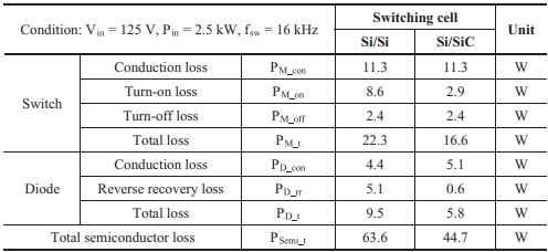
Table II. Loss breakdown of semiconductors in IBC at critical condition
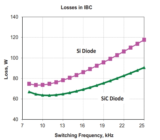
Fig 3. Losses in the IBC with switching frequency variation
Fig. 3 shows the calculated system losses of the IBC using the two different diodes under study and the operating switching frequency as a running parameter. Through the optimum inductor design procedure, the optimal switching frequency for Si and SiC diodes are found to be 10 kHz and 11kHz, respectively. However, a minimum switching frequency of 16kHz is set to avoid generating acoustic noise. As such, the inductors are the same in both cases as well.
The cooling system for each IBC was designed in order to maintain the junction temperature of CoolMOS at 75°C and the ambient temperature at 50°C. Different sets of fan arrays are used to maintain ambient temperature. The heatsinks were made using the same material but with different lengths and fin heights in order to maintain similar operating parameters. As a result, there is a 60% reduction in dimensions of the Si/SiC system as compared to the Si/Si system.
Ⅱ. Experimental Verifications and Results
To determine the difference between the Si/SiC system and the Si/Si system, the authors performed efficiency characterization studies for a PV inverter, which includes MPPT efficiency and static converter efficiency. Since the dynamic response of the semiconductors is considerably higher than the MPPT control bandwidth, using either Si or SiC diodes does not impact MPPT efficiency.
To characterize static efficiency, a PV simulator and a dc electronic load were connected to the IBC under test. The duty ratio for the IBC is manually assigned using an open-loop controller. Both European efficiency and CEC efficiency were measured using a power analyzer.
The results of the tests were as follows:
1. The junction temperature of the Si diode is 17°C higher than the SiC diode. This is because of the Si diode's higher switching loss and the heatsink's lower thermal resistance in the Si/Si system.
2. The junction temperature of the CoolMOS devices in the Si/Si system is slightly higher than in the Si/SiC system.
3. Both systems show higher efficiencies at high voltage and high power operations due to reduced semiconductor losses and inductor core losses. However, efficiency deteriorates in low-power and low-voltage operations.
4. In both European efficiency and CEC efficiency, the Si/SiC system is better than the Si/Si system by 0.4-0.8%.
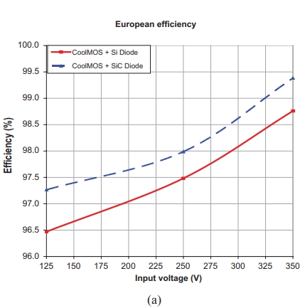
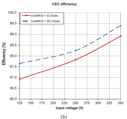
Fig 4. The efficiency of the IBC: (a) European, and (b) CEC
Table III shows that the Si/SiC system outperformed the Si/Si system in terms of efficiency, volume, and weight. The Si/SiC system provided a significantly higher efficiency and a higher power density through only a one-to-one diode replacement and system optimization.
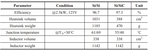
Table III. Summary of comparisons of Si/Si vs Si/SiC systems.
- Prev:None
- Next:What is the Difference between DCS and PLC?
Suggested Resources
-
Phone
18126161077 -
Wechat

